Work Package Structure
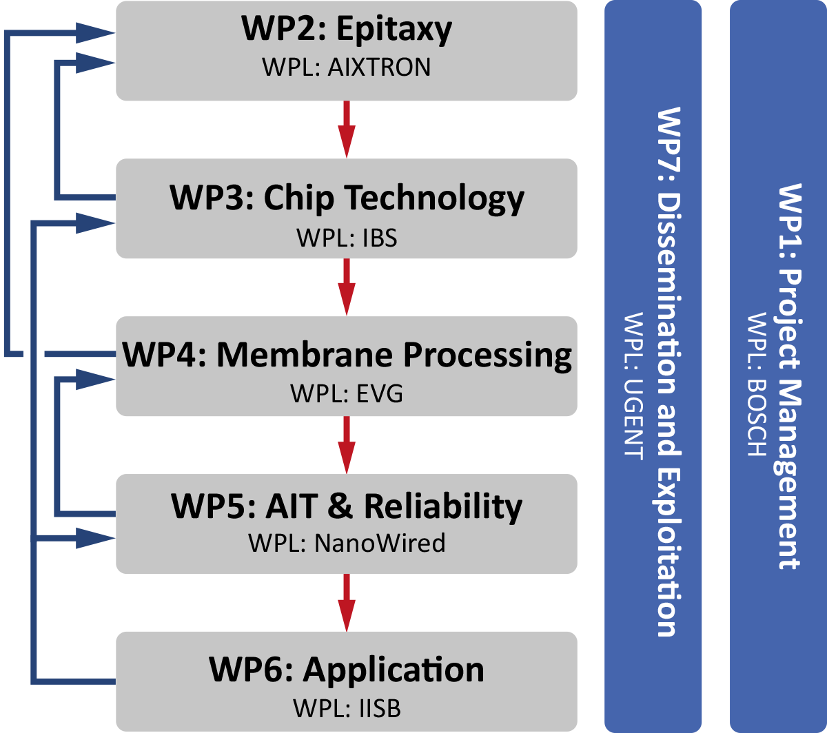
WP1 – Project management
Lead: BOSCH, Participants: AIXTRON, Fraunhofer, EVG, IBS, X-FAB Global, NanoWired, UGent
– Timely and efficient implementation of the work plan
– Continuous monitoring of all project activities
– Management of project scope and objectives
– Communication management within and outside the project
– Management of risks, innovation and quality
WP2 – Epitaxy
Lead: AIXTRON, Participants: FBH, CNRS, SOITEC BE, Fraunhofer, Hexagem, ULUND, UVEG, UGent, SILTRONIC
– Development of an industrial epitaxial technology to fabricate vertical device layer stacks
– Provide the required epitaxy stacks to WP3 (chip technology) for further processing
– Development of a fast characterization scheme for the epi layers
– Development of equipment for GaN epi on Si wafers and material performance
– Exploration of the use of nanowire reformation layers to reduce stress management efforts
WP3 – Chip technology
Lead: IBS, Participants: Bosch, FBH, CNRS, Fraunhofer, EVG, ULUND, X-FAB Dresden, UVEG, UGent, IUNET, ST-T
– Development of vertical GaN power transistors with up to 100 A current and 1200 V voltage
– Development of different transistor architectures including MOSFETs and FinFETs
– Development of basic processing modules suited for mass manufacturing
– Development of ion implantation technology and equipment for Mg implantation
WP4 – Membrane processing / backside access
Lead: EVG, Participants: Bosch, FBH, CNRS, IBS, X-FAB Global
– Development of crucial processing technologies enabling backside access to vertical device structures and subsequent backside processing of device wafers
– Development of advanced bonding and debonding technologies enabling processing of fragile wafers, local substrate removal of silicon, sapphire substrate lift-off as well as ohmic contact formation and backside power metallization
– Scaling and industrialization of the processes and the equipment
– Manufacturing of test and device wafers both on Si and on sapphire
WP5 – AIT and reliability
Lead: NanoWired, Participants: Bosch, Fraunhofer, UVEG, MCL, AUREL, ST-T
– Assembly & Interconnection Technology (AIT) as well as corresponding reliability characterization for the power transistors developed within WP2-WP4
– Creation of extensive knowledge on physical, reliability and cost constraints of the possible AIT solutions
– Demonstration of innovative technologies such as Nanowires, Cu-Sintering, embedding technologies, direct bonding and step substrate approaches as well as established interconnection techniques such as silver sintering, wire bonding and ribbon bonding
– Device and reliability characterization of the developed power switches
WP6 – Application
Lead: Fraunhofer, Participants: FBH, FPG, SiCtech, AUREL, IUNET, Raw Power
– Creation of a technical data sheet for the new vertical GaN power transistor
– Demonstration of the advantages of vertical GaN membrane transistors in terms of system efficiency, power density and cost effectiveness for high power converter applications with medium and high switching frequencies
– Setup of system simulation environment (Digital Twin) to evaluate the new GaN devices and their impact on system level
– Design and development of a high performance WBG half-bridge power module, which will be applied to realize application-specific system demonstrators to evaluate the benefits of the new devices on application respectively system level
WP7 – Dissemination and exploitation
Lead: UGent, Participants: all partners
– Plan, coordinate and execute dissemination activities to the scientific and industrial communities
– Ensure a visible impact of YESvGaN both at the EU and world-wide
You can find us on

